What are the Common Parts of a PCB?
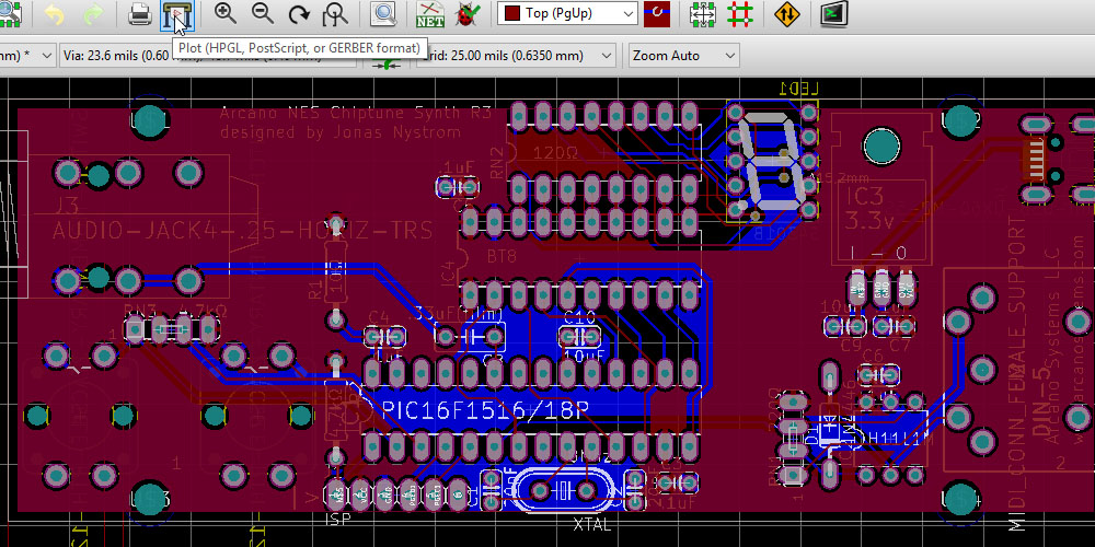
A printed circuit board is an important part of an electronic device. It comes in different forms and is designed using different design processes. During the creation process, you can view the various parts of the PCB in 3D through the help of a KiCad tool. Click on KiCad Gerber to learn more about the tool and how to export the standard Gerber file from KiCad after completing the design process. In this write-up, we expound on the different parts of PCB below.
Common Parts of PCB
The design and components of PCBs vary depending on their use. Some have more components than others, while some designs are more intricate than others. However, there are general parts common in most printed circuit boards that we will discuss below.
1. Layers
PCBs are constructed with different layers such as single, double, and multiple layers. The single-layer PCB is the simplest to design and construct and is mostly used in daily routines. The double and multiple layer PCB have complex designs and are used in large and heavy circuits. The layers are connected via a hole using a wire, ensuring communication is maintained between all components.
The number of layers you would like your PCB to have is influenced by the cost, application, and size of the circuit and components. Fewer layers mean fewer components and vice versa.
Other than the layers within the PCB, the top and bottom layers are also crucial parts of the circuit board. The top layer or the component layer is known for providing mounting space and acts as the base of the electronic components.
When you disassemble most electronic devices like radios, mobile phones, or cameras, you will find that this PCB layer is green, but there are few exceptions. The bottom layer or the solder layer offers a spot for wiring and soldering of components.
2. Pad
The pad is a piece of copper mostly found on the top and bottom layers of a printing circuit board. It offers all components the needed mechanical support since it is where mounting and soldering takes place.
3. Trace
A trace is a track that conducts electricity on the printed board circuit and allows it to flow to all the electric components with very little resistance. Any material that conducts electric current can be used as a trace, but copper is used in most cases.
4. Silk Layer
This part is also known as silkscreen and is used to mark out any electronic feature on the circuit board. It allows printing whereby epoxy ink is applied, art, or any text on the PCB surface. The silk layer can be found at the top, bottom, or both layers of the PCB, depending on the client’s requirements.
5. Solder Mask
This part of the PCB acts as the insulating layer to prevent excessive heat from reaching any component. It stops any contact between the copper pads and any material that conducts electricity.
Final Word
Above are the main PCB parts that play a significant role in its operation. Some parts are standard, while others can be changed based on your requirements to fit your applications. The printed circuit board is essential in all electronic devices; hence all its parts should function well.